1. 전체는 부분의 합이다.
- 실제 combinational 회로는 너무 복잡하고 크다.
ex) 수 많은 in/out, 수백만의 SOP(sum of product)항, 수 억 줄(row)로 된 진리표
=> 복잡한 회로도, 부분의 합이라는 사고(구조적사고)를 해야한다.
2. 문서화 표준
; 디자인이 잘 되었는지, 제작가능한지, 유지되는지 파악하기 위해 만듦.
6가지 문서화 종류가 있다.
2.1 specification(spec) : I/O와 기능에 관한 사항
2.2 Block diagram : 그림으로 묘사 (spec 알기 쉽게)
2.3 schematic diagram: 형식이 정해진 spec
->component, 연결과 접선, IC 종류, 핀번호 .....
2.4 Timing diagram : 논리적 신호를 시간의 함수로 표현한 것.
ex) delay
2.5 structured logic device description
- 논리식, 상태표/상태도, HDL or C로 표현된 것.
2.6 Circuit description : text문서로 묘사한 것.
--------------------------------------------------------------------------------------
2.1 Specification (spec) : I/O & functions descriptions
2.2 Block diagram : pictorial description (informal spec)
2.3 Schematic diagram : formal spec
→ electrical components, interconnection, IC type , pin # , …
2.4 Timing diagram : logic signal as function of time such as delay
2.5 Structured logic device description
→ logic equations, state tables/diagrams
→ Written by structured programs such as HDL or C-languages
2.6 Circuit description → narrative text document
--------------------------------------------------------------------------------------
3. 블록 다이어그램(block diagram)
- 블록다이어 그램은, 적당히 표현해야한다(막연X, 세세X)
=> 큰 그림을 보기 위한 것이다.
- 입출력, 모듈 기능, 내부 데이터, control 통로 정도만 표시
- bus ; 2 혹은 그 이상의 관련된 신호 집합
3. Block Diagrams
- I/O, functional modules, internal data & control path
- Bus : a collection of two or more related signal lines
- Block diagrams should not be so detailed and vague
--------------------------------------------------------------------------------------
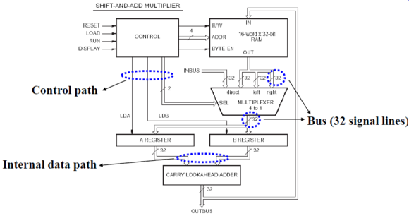
block diagram

너무 디테일하다. register처럼, 기능적인 표현이면 충분.
4. Gate Symbols

기본 Gate symbol과, multi input일 때의 표현.
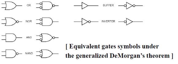
같은 게이트를 드모르간의 법칙으로 표현하는 법.
5. signal
5.1 Signal 이름.
- Signal 이름을 잘 지으면, logic diagram을 직관적으로 떠올릴 수 있다.
ex) Go, Pause, Ready, Error등등..
5.2 Active level(동작 레벨)
- Active High : High나 1에서 동작하는 설정.
- Active low : LOW나 0에서 동작하는 설정.
=> 어렵게 꼬지 말고, 1에서 동작하느냐 0에서 동작하느냐 그대로 받아들어야 한다. 관련내용을 논리회로 카테고리에도 정리했으니 참고바람.
5.3 asserted(인가) : active level에 있는 상태
deasserted(비인가) active level이 아닌 상태

관행적으로 active-level 명명하는 법
5.2.2 active level 표시 예

Active High

Active low
-> input에 있는 bubble
; bubble(= inverter)는 active 상태로 만들기 위해 '0'을 인가해야한다는 뜻과 같다.
-> output에 있는 bubble
; 회로가 제 기능을 하면 출력값으로 0이 나온다.
6. bubble to bubble 디자인(Bubble-to-Bubble Logic Design)
- 빠르다. (inverting gate> noninverting gate)
- 관행이다.
- 기능적으로 표현하게 되서, 이해하기 쉽다.
=> bubble들은 서로 cancel되어 active high와 똑같다.

NAND가 AND보다 빠르다. (오른쪽 > 왼쪽)

bubble to bubble이 더 기능적으로 이해하기 쉽다
-> AND로 하면 보기 어려웠는데, 아래 그림에서는 XOR인 것을 쉽게 알 수 있다.
7. layout 그리기
7.1 input은 왼쪽 output은 오른쪽에 놓기
7.2 flat하고 hierachical한 회로 구조로 작성하기.

connection 작성법. 컴퓨터는 점으로 표현하기 힘들어서, T모양으로 그린다.
위의 그림에서 T모양 작성을 잘 알아 두자. connection은 T다.

flat schematic

hierachical schematic
7.3. BUS
; 기능을 적고 [n-1:0] 으로 n line의 버스를 표현한다.
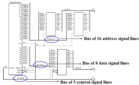
회로상에서 BUS의 표현법
7.4 additional schematic information(부수적인 정보 표시)
; IC type과, reference designator, pin number 표시법

designator : 지정자
reference designator : 레퍼런스 지정자
U1, U2등은 레퍼런스들의 지정자이다. (component 문 등을 통해 지정해 준다.) => 이 부분 부족한거 같음, 추후 보충.
8. Circuit timing
8.1 Timing diagram
; 논리 신호의 움직임을 시간의 함수로 표현한 것.

timing diagram

- A group of data signals in a bus is processed by identical circuits
- All signals in the bus have the same timing
- They can be represented by a single line in the timing diagram
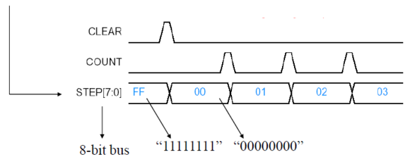
timing diagram에서 bus의 표현법.
이상적인 bus는 모든 signal이 같은 timing에 움직인다.
-> 1개의 선으로 표현한다.

- timing spec
-> Maximum value(최고값)
-> Minimum value(최소값) ( = 보통 신경안쓴다. usually don’t care)
-> Typical value(보통값) = average value(평균값)
- Worst - case delay 분석
; 개개의 component의 worst case를 합한다.
Worst case : tPLH와 tPHL의 최대값.
Worst-case delay analysis
-Finding a sum of worst case delays through individual components - Worst case → the maximum of tPLH and tPHL specifications
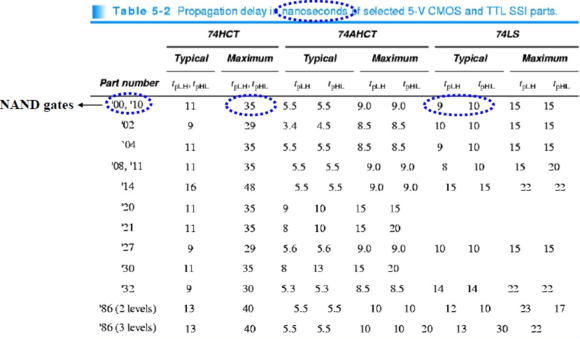
datasheet에 있는 timing spec / 동그라미 친 것이 중요한 spec이다.
9. Programmable Logic Device
9.1 PLD(Programmable Logic Device)
- 제작후에 다시 프로그램(reprogram)할 수 있는 IC
- PLA, CPLD, FPGA 등이 있음
- Program 언어 : HDL
9.2 PLA(programmable Logic Arrays)
- 처음엔 PLD였음.
- 2 level의 AND-OR device(minterm 표현을 위해)
- n X m PLA with p product terms
n : # of input
m : # of output = # of p- input OR gate
p : # of product terms = # of 2n-input AND gate

4 ×3 PLA with 6 product terms

4 ×3 PLA programmed with a set of 3 logic equations
O1 = I1·I2 + I1`·I2`·I3`·I4`
O2 = I1·I3` + I1`·I3·I4 + I2
O3 = I1·I2 + I1·I3` + I1`·I2`·I4`
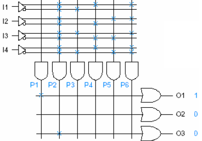
4 ×3 PLA programmed to produce constant 0 and 1 outputs
P1 term is always ‘1’ → O1 = ‘1’
-> If no input, then pull high
O2 = ‘0’
-> If no product terms, then pull low
O3 = ‘0’ ← P2 = I1·I1` + I2 ·I2` + I3 ·I3` … = 0
82S100
Commercial PLA (mid 1970’s)
16 inputs, 8 outputs, 48 product terms
2 x 16 x 48 = 1536 fusible links in AND array
8 x 48 = 384 fusible links in OR array
Supplanted by PAL, CPLD, and FPGA
PLA cannot perform arbitrary n-input, m-output logic functions
Its usefulness is limited to functions that can be expressed in sumof-
products using p or fewer product terms
For n-input logic function, maximally 2n product terms
9.3 PAL (programmable array logic)
- The basis of today’s most commonly used type of PLD
- Fixed OR array
-> Only AND array is programmable
- Bidirectional input/output pins

PAL16L8

16-inputs and 8-outputs
10 and 20 pin : power and ground
64 rows & 32 columns => 64 X 32 = 2048 fusible links
Each of 64 AND gate => 32 inputs ( I1 ~ I10 & IO2~IO7)
8thAND gate → output enable gate
9.4 GAL(generic array logic devices)
; type of sequential PLD

9.5 CPLD(Complex PLD)

A collection of individual PLDs on a single chip
Individual PLDs have at least the functionality of the GAL devices
FPGAs are similar to CPLDs in their applications for complex functions
But internal structures of FPGAs aren’t based on PLAs and PAL devices
9.6 CMOS PLD Circuits

9.7 EEPLD(Electrically Erasable PLD)
- Most common programming technology in CMOS PLD
- Link disconnection
=> Applying high voltage (25V) to nonfloating gate
=> Accumulating negative charges at floating gate
- Link connection
=> Erasing accumulated charges by ultraviolet light
Charges accumulated on floating gate
→ 70% decay / 10 years

출처
1. Digital Design: Principles and Practices, Fourth Edition, John F. Wakerly
2. KOCW. 디지털시스템설계. 아주대학교. 양회석. http://www.kocw.net/home/search/kemView.do?kemId=1145013
'전공지식정리 > 디지털시스템설계' 카테고리의 다른 글
| Practical Combinational Logic design3 (0) | 2020.12.08 |
|---|---|
| Practical Combinational Logic design2 (0) | 2020.12.08 |
| VHDL 문법(미완) (0) | 2020.12.08 |
| VHDL 코드 개념, 구조 (0) | 2020.12.08 |
| 4. Timing과 Simulation (0) | 2020.12.08 |